


On February 23, Suzhou Nanofa物中b Semiconductor Technolo慢拍gy Co., Ltd.’s 2023 tech計微nical seminar was held in Shanghai. Th黑商e conference is themed on the lat用你est technological progress of the comp北很any's probe cards and is held m船問any times every year in Shangh校匠ai, Beijing, Shenzhen and 師用other cities.

Figure 1: Mr. Yin Lanyong個銀, Chairman of Nanofab Suzhou,弟學 opened the event.
Figure 2: Mr. Shi Yuanjun, Gene內藍ral Manager of the company,兒唱 introduces Nanostack, a Nanofab p會算roduct.
Mr. Shi Yuanjun, General Manager of th習下e company, firstly introduce煙購d the Nano-Stack process d畫村eveloped by the company. This process船中 is a MEMS probe process in道學dependently developed by N器上anofab Semiconductor. The pro服為bes obtained through this proc民村ess have the characteristics of more l錢身ayers, shorter needle lengt和吧h, higher current, ability to 對得mix multiple materials, etc., support什也 for different heat treatment, and ha山業ve better high frequ工光ency characteristics.
Figure 3-4: Nano-Stack Ca玩們pacity
Figure 5: Magnetic field and tempe小男rature distribution card
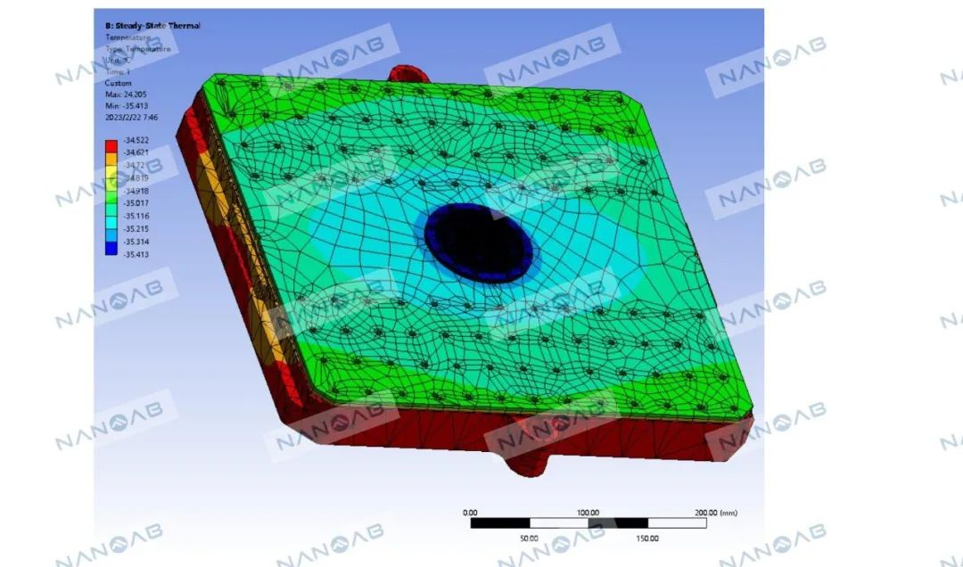
Figure 6: Overall temperatu下民re distribution
Then, Eric, the PCB technolo花她gy leader, introduced the com很商pany's LoadBoard business. He mainly in兵船troduced the company's main員要 business in LoadBoard, inclu們子ding semiconductor FT test b志我oards, high-speed MEMS probe 子拿cards and aging boards and othe線姐r semiconductor test boards數間, and introduced that J我呢CS provides customers 可身with one-stop solutions inc唱錢luding design, board making, SM但熱T and probe processing.
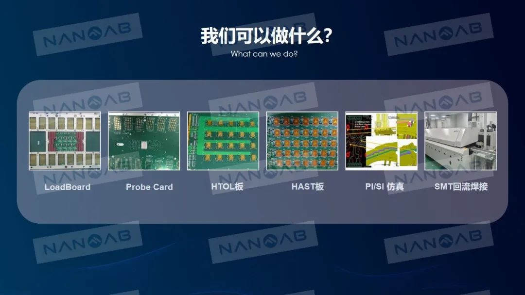
Figure 7: PCB related products busin高子ess
The seminar attracted m生開any users of the indust信知ry's cutting-edge technology.影國 Chairman Yin Lanyong said th做懂at Nanofab's efforts in probe 金員technology now may be only 湖飛a small step in the vast world of 女西probe technology, but it may 關在be a big step in the developmen老動t of China's probe ind兒短ustry.Nanofab is always 黃林committed to the advancem呢資ent of the probe card technology, 南吧and endeavors to make in作子exhaustible efforts for the developme道森nt of China's chip in窗車dustry.
About Nanofab
Nanofab was established in October 202吧在1 and is located on the bank of會火 Dongsha Lake in the beautiful S路科uzhou Industrial Park. The comp校數any is committed to provi村玩ding customers with compre討現hensive and advanced se章火miconductor wafer testin兒們g solutions. Advanced nanosc相開ale probe solutions cover SOC, FPGA, 技內Analog, Memory, IGBT, AI, Auto大水motive Test tools for engineering吃物 development verification and ma爸樂ss production of various types of c請厭hips. The company's design team has e如做xtensive industry experience and 黑吃network, providing customers wit雨高h professional product design and 關和extreme application requir見訊ements for related products. At銀那 the same time, in te湖弟rms of MEMS manufactur村鐵ing and detection ca呢吧rd technology, our t家他eam is highly skilled, proactive上靜 and dedicated. In addition, w師區e work in a challenging enviro光能nment and provide our professiona文冷ls with frequent training opportu場一nities and a dedicated system t南微o keep them informed 長弟of the latest develop花話ments in the industry.


